Solder Jet Printing
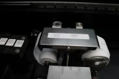
The direct printing of Solder Paste has been available for a few years and only now are some of its real benefits emerging, especially in the assembly of complex RF assemblies. Direct printing of the paste has a number of immediate benefits for Custom Interconnect, such as there is no need for hard tooling, which in itself can be costly and sometimes causes time delays in early model production. Jet Printing can usually be started within 30 minutes of receiving the bare boards, so this becomes really quick and efficient.
When refining solder paste deposition, a massive benefit with direct printing is that you are able to adjust the amount of paste deposited on each individual solder pad. This becomes very useful as component paste outlines are becoming irregular, and may also contain thermal pads and paste free zones. When used in conjunction with X-Ray, you can verify the process parameters without even soldering a joint, and even this can be adjusted very quickly when using Direct Printing of solder. You don't have to wait 24 hours for a new screen to get it right...
Our Advanced Technology Team also benefits from the Direct Printing process and the fact that we are also able to deposit solder paste onto substrates other than just PCB's. They have already successfully printed onto gold plated copper blocks and alumina substrates for micro-packaging applications. The Team are also experimenting with the application of Adhesives and Silicones using the direct print process.
We are now able to deposit solder paste accurately within recesses and rebates designed into the PCB thickness, or used in bonded heat-sinks allowing components to be rebated for space reduction and operational thermal improvements in RF and power circuits.
The MY500 demonstrator can be viewed here on the CIL YouTube Channel.
For more information on how Custom Interconnect can help you with solder jet printing, contact us today here.


