Bringing semiconductor packaging back to the UK
As geopolitical tensions proliferate, relying on Far Eastern semiconductor component imports becomes riskier than ever. Here’s how one UK electronics manufacturer has used advanced technology to mitigate the problem.
In Europe, we have all grown up in an environment where importing semiconductor products, subassemblies and components from Far Eastern suppliers seems inevitable, since their staffing and manufacturing costs have been so much lower than ours. This approach has always been expedient rather than ideal, but escalating worldwide tensions are ramping up our supply chain vulnerability to unacceptable levels.
Problems and threats in Eastern Europe, the Middle East, the Red Sea and China mean that component sources could disappear, or that trade routes may become excessively slow, expensive, or simply unavailable. Therefore, governments and industry leaders are exploring domestic self-sufficiency in material supply and manufacturing.
In Europe, the EU has introduced the European Chips Act, designed to address semiconductor shortages and strengthen Europe’s technological leadership. It will mobilise more than €43 billion of public and private investments and set measures to prepare, anticipate and swiftly respond to any future supply chain disruptions[ii]. Similarly, the Biden administration in the US has introduced the CHIPS and Science Act, which provides $52.7 billion for American semiconductor research, development, manufacturing, and workforce development.
Unfortunately, the European Chip Act’s funding and opportunities do not extend to the UK. However, this has not stopped pioneering electronics manufacturer Custom Interconnect Limited (CIL) from making a major new investment into the plant, equipment, and staff needed to back the concept.
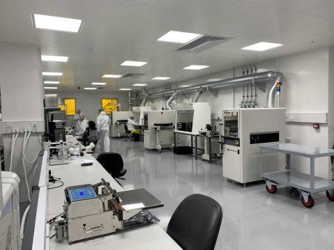
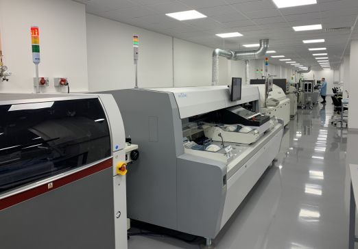
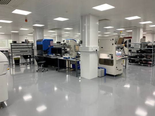
With over 36 years of electronics assembly experience, the company has just opened an entirely new 64,000sq ft site; known as BP2, it houses the largest semiconductor packaging facility in the UK. This highly automated factory includes both a volume PCBA production area and a 15,000sq ft semiconductor packaging ISO 7 clean room. All of this is in addition to CIL’s long-established production area in CIL House.
Bringing semiconductor manufacturing back to the UK
The semiconductor assembly clean room contains a segregated area with specialist LED lighting, to house CIL’s wafer dicing capability complete with dicing saw, water treatment and wafer mounting equipment. The BP2 site operates with bidirectional flow between PCBA production and semiconductor packaging.
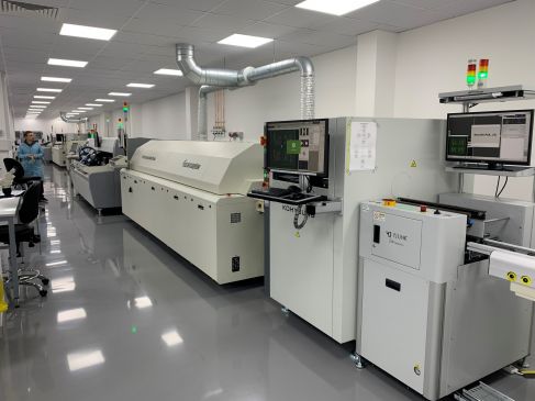
In one direction, a Chip on Board (COB) PCB progresses through the PCBA manufacturing process, with SMT components being assembled onto the board with in-line 3D Automatic optical inspection (3D AOI). The PCBA is then moved into the semiconductor assembly area, where the bare dies are mounted on the PCBA using a conductive or non-conductive epoxy and then wire bonded. The methods used for wire bonding are Au Ball, Al Wedge and for RF devices Au Wedge. CIL has all three technologies and sometimes has to mix wire bonding technologies on the same assemblies, due to die type. Wire counts vary from a single wire bond up to 1000 / device and CIL currently performs approximately 1.5M wire bonds / week. These wire bonded die are then 100% encapsulated (glob top), part encapsulated, or left completely exposed.
The completed PCB can then be inspected and shipped out to the customer.
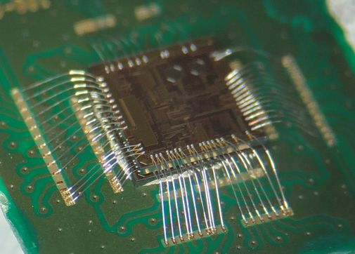
CIL Chip on Board Assembly
In the reverse scenario, a wafer dicing/sawing process within the semiconductor packaging clean room is used to singulate wafers into individual die. These can then be sorted into waffle/GEL packs, and shipped to the customer. Alternatively, they can be wire/die bonded onto a leadframe and then go through CIL’s plastic overmold process. These completed custom QFN SMT packages are then separated and moved into CIL’s SMT assembly area for SMT placement onto their respective PCBA. In this instance the customer is supplying custom wafers, and CIL is performing the full packaging and PCBA assembly service, all within the UK.
Wafer substrates of up to 300mm diameter can be sawn, and multiple wafer types, including silicon (Si), gallium arsenide (GaAs), gallium nitride (GaN), glass, and ceramics are supported. CIL has become a semiconductor manufacturer as well as an electronics PCB assembly specialist.
The new BP2 site’s high-volume production capabilities are complemented by the established CIL House facility, which houses a dedicated rapid prototype SMT PCBA line and a further five production SMT PCBA lines for small to medium volumes of complex PCBA assemblies. The combined facilities allow CIL to support customers throughout their entire product lifetime, from initial concept development and prototyping, through early low and medium volume production runs, and on to full high-volume production for as long as required.
CIL is involved in these processes very much as designers as well as prototype and volume manufacturers. In one major project, CIL is the project lead on GaNSIC - a project that stems from the UK Research and Innovation’s (UKRI) ‘Driving the Electric Revolution’ challenge[i] and brings together CIL and Compound Semiconductor Applications Catapult (CSA Catapult). It is set to develop novel ways of applying Silver Sinter pastes to wide band-gap (WBG) semiconductors such as silicon carbide (SiC) and gallium nitride (GaN) devices to optimise their thermal coupling and solve complex power module assembly challenges. WBG semiconductors are finding their way into EV battery switching systems because they can handle the very high power densities involved. However, producing assemblies that perform reliably depends on some novel and advanced manufacturing and inspection techniques, which have been developed by CIL in partnership with their suppliers. The company has also been engaged in further development to maximise potential for future battery EV systems, working with BMW’s Advanced Propulsion Centre on a project named APC15@FutureBEV and JLR on project EleVAIT. In addition to these funded projects, CIL is also working 100% commercially on a growing number of WBG power projects. Increasingly CIL finds itself designing, developing and producing these assemblies for its customers.
Also, in early 2021 CIL became the semiconductor assembly partner for a Department for Science, Innovation and Technology (DSIT) project OranGaN. This project brings together lead partner INEX Microtechnology, and CIL with Viper RF and Compound Semiconductor Applications (CSA) Catapult. The project is developing new manufacturing processes and packaging solutions to create 5G components such as Monolithic Microwave Integrated Circuit Chips (MMIC). Currently, there are no commercial RF-GaN devices fully developed and manufactured in the UK that can be used in 5G applications. MMIC chips are used in power amplifiers— components that boost signals before they are transmitted from a base station to smartphones and computers. CIL's participation in the project was to develop QFN style packaging including die attach, wire bonding, plastic overmold, device separation and marking for devices operating at up to 40GHz.
All CIL’s OEM customers are engaged in delivering advanced technology products into demanding applications such as EVs or medical instrumentation. Although volumes are not as high as for consumer applications, they can still be considerable – The single double sided PCBA assembly line at BP2 is already placing 6 million components a month, with a first time pass rate >99.4%. Of the 6 million components, 5 million of them are 0201 passives, so highly complex assemblies. As it is for a medical application, the entire assembly has to have 100% traceability. CIL records for a single PCBA assembly, every component used, 3D AOI results, in respect of the die, and wafer, die and lot numbers of all process materials consumed down to a single board. To achieve this, everything is bar coded and CIL relies on all of its latest assembly machines to read barcodes before progressing.
What are the factors involved?
So how is CIL competing so successfully with Far Eastern suppliers in delivering very complex, high quality components and assemblies in large quantities and on time – and, above all, competitively?
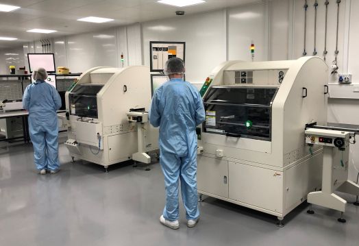
Primarily, the answer lies in very high levels of automation. When a production line needed 20 technicians on European wages to operate successfully, the wage bill ruled out competitiveness with the Far East. But this problem becomes insignificant at CIL’s level of automation, where a complete line is run by just two operators. While critically reducing labour costs, automation has also vastly improved throughput – from 500 hand- built semiconductor assemblies a week to a current automated rate of 4500 a week.
Other key aspects are product quality, and machine reliability and uptime; but these depend on both the machines and their suppliers. Chances of inadequacy or failure can be greatly reduced by investing in high quality equipment, but it’s an inescapable reality that no machine is completely immune to failure. If a failure does happen, the supplier’s response is critical. With downtime costing £80,000 per day, plus risk of reputation damage, repairs must be made in minutes or, at the worst, hours. Waiting weeks for a spare part to arrive is completely unacceptable.
Additionally, suppliers play a crucial role in ensuring that CIL staff are correctly trained and supported, so they can always coax optimal performance out of their production lines.
CIL has also simplified their drive to shorten supply lines and bring semiconductor manufacturing back to the UK by consolidating suppliers. The production, testing, and inspection machines they buy are by necessity advanced technology and complex, so finding and managing numerous suppliers who can offer and then deliver and support suitable solutions is challenging. Conversely, a supplier who can offer all the manufacturing and inspection equipment across a production line is well placed to understand how the machines are interacting with one another, and optimise the process accordingly. For example, X-ray or acoustic microscope inspection results could be used to modify reflow profiles and whether time above liquidus should be extended to reduce voiding.
The IPP Group: broad range and deep expertise
The IPP Group not only ticks the above boxes, but has also been supplying CIL for 16 years. Accordingly, it was in a pole position to help with their expansion plans. The Group has delivered Nordson Asymtek automated precision fluid dispensing systems for glob top encapsulation with very tight tolerance during semiconductor assembly, as well as Vitronics Soltec reflow soldering ovens for the PCBA lines. These are drawn from their range of SMT and post-SMT manufacturing equipment, materials, and consumables for electronics production lines, and backed by their 40 years’ experience of process development and installation.
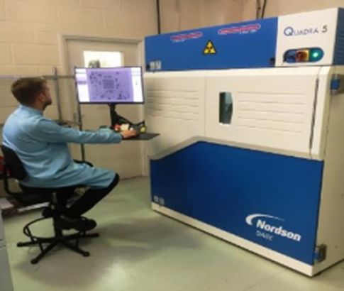
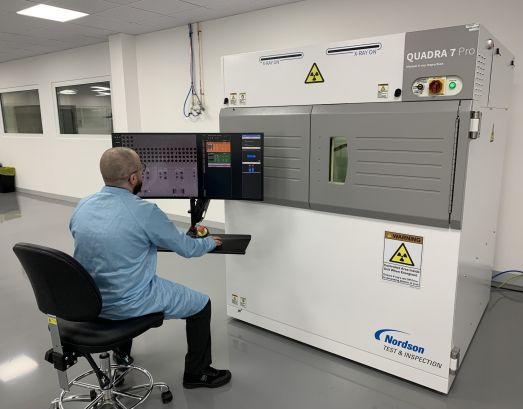
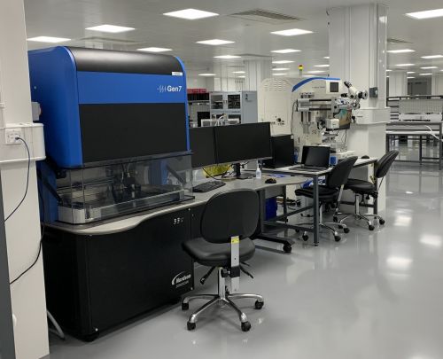
For inspection, CIL has purchased a Nordson Dage QUADRA 5 X-ray machine plus a Nordson SONOSCAN Gen7 SAM acoustic microscope previously, and a new QUADRA 7 Pro X-ray machine, all from Cupio Ltd – originally an independent inspection equipment specialist, but now part of the IPP Group. In fact, the QUADRA 5 / 7 X-ray – with CT scan capability - and CSAM acoustic microscope add up to an integrated inspection capability which uniquely allows CIL to reliably perform their high-precision silver sintering die attachment process, used in manufacturing WBG semiconductor assemblies. The SAM’s high resolution complements the QUADRA 5 / 7's imaging detail.
Cupio Services (CS) investigates issues within components as well as SMT mounting problems. For example, they can check for delamination, BGA balling, and broken wires inside components as well as PCB tracks and component to PCB connections. Root cause analysis is possible, even for equipment not supplied by IPP.
CIL can also send suspect components to CS for dissection and deeper analysis. Additionally, CS can help with sampling for reliability analysis, and to spot potential failures. Lifetime testing is also possible.
Expanding the initiative into the future
John Boston, Managing Director of CIL, comments: “CIL’s ultimate strategy is to maximise and optimise our offering of prototype, small-, medium-, and high-volume PCBA and micro-electronics/power device assembly, all from one company. We have a planned growth trajectory across diverse industries and market conditions.
“Expansion will continue, with two more SMTA production lines planned for BP2 in 2024, and further development in 2025. Also, over the coming years we will be adding further semiconductor packaging technologies and processes to give our customers the technological lead they need to be successful.
“I’m looking forward to continuing our close relationship with the IPP Group. We have built up solid relationships with their key staff, and trust their expertise and commitment to delivering on their promises.
“We turn to them not only for supply of new equipment, but also for their valuable training and advice on how we can continue improving and getting the most out of our production and inspection equipment capabilities. Now, the consolidation of the IPP Group and Cupio Ltd will make both purchasing and technical support more efficient and easier to manage than ever.
“Overall, we are very proud of our BP2 investment, and how it is allowing us and our customers to counter the ever-increasing worldwide threat to our supply chain integrity. We also believe that our story will be encouraging to other UK electronics manufacturers, as we have proved that it’s possible to reduce dependence on overseas semiconductor suppliers.”
References
[i] https://csa.catapult.org.uk/2021/01/06/custom-interconnect-ltd-and-compound-semiconductor-applications-catapult-drive-electric-transport-revolution-with-developing-novel-ways-of-depositing-silver-sinter-paste-for-wbg-applications/
[i] The supply chain trends shaking up 2023 - KPMG Global
[ii] European Chips Act - European Commission (europa.eu)
[iii] FACT SHEET: CHIPS and Science Act Will Lower Costs, Create Jobs, Strengthen Supply Chains, and Counter China | The White House
