Custom Interconnect Ltd invests £9M and expands with a new Semiconductor packaging, power device and PCBA manufacturing facility in Andover, UK


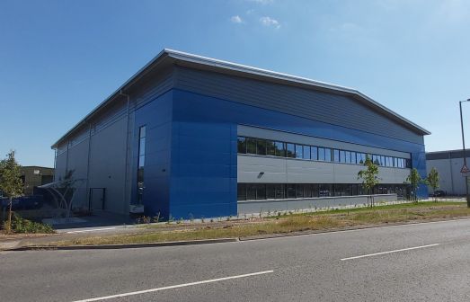
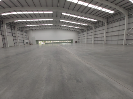
CIL is excited to announce that it is creating an advanced semiconductor packaging, power device and volume PCB Assembly (PCBA) manufacturing facility in the UK. Supported by £9M in capital investment the 46,000sq ft is in addition to its existing 34,000sq ft, giving CIL over 80,000sq ft in Andover, UK. Following the first stage six-month fit out of its ISO7 (Class 10,000) cleanroom totalling 15,000sq ft and associated offices, all of CIL’s micro-electronics production and power device development will relocate to the new facility in March 2023.
CIL has seen very strong demand for its micro-electronics and electronic assembly capability through the COVID period. Coupled with its InnovateUK supported innovation programs that are focussed on strategic areas including power device development and compound semiconductor technology, CIL has generated the demand for this investment in increased capacity and capability.
Starting with InnovateUK joint funded project “GaNSiC” in 2019 and then followed by APC15 project “@FutureBEV” in 2020, CIL has been supporting the development of GaN and SiC based power modules, discrete devices and associated power PCBA. These two projects have been catalysts to significant further R&D projects that have been supported by national funding programs including the Advanced Propulsion Centre (APC), Driving the Electric Revolution centre (DER-IC), DCMS and InnovateUK. They are all focussed on more efficient power electronics in support on Net Zero. The technologies span a range of sectors including automotive, rail, aerospace and space, 5G Communications and data-centre infrastructure. Since 2019, CIL has increased its specialist engineering department from 8 to 30 engineers with further plans to double it again over the next 3 years. This investment in engineering skills coupled with the additional unique processing equipment, will create one of the UK’s largest independent semiconductor packaging facilities, and will accommodate both world leading development labs and full volume production areas. The UK has a thriving Integrated circuit (IC) design community, but very little UK based packaging capability able to deal with development, low volume and high-volume production, the new facility is the first stage in CIL addressing this capacity requirement.
As well as the additional capacity, CIL is also increasing its process capability as it adds equipment such as a DISCO DAD 3361 dicing saw, Boschman UNISTAR Automatic Film Assisted Plastic Overmold and Scheugenpflug VDS U1000 / LP804 VDU Auto epoxy fill system with more to equipment and processes to come. Once commissioned, this equipment will enable CIL to offer UK-based wafer dicing, full device overmold service for devices such as QFN’s etc, partial device overmold and SiC and GaN based power module potting manufactured within a UK-based, UK-owned facility.
By March 2023 the stage 1 fit out will be complete and CIL will then relocate its micro-electronic production and power module and device development to this new facility, which will include the following:
- 2 off DATACON 2200EVO Automatic die bonders
- 2 off HACKER Automatic die bonders
- 2 off Manual die bonders including Eutectic soldering
- 5 off ASM 589 Auto Al wedge bonders
- 2 off ASM EAGLE60 Auto Au Ball bonders
- 1 off K&S Asterion Heavy Gauge Wedge wire bonder
- 1 off DAGE 4000 die shear and wire bond pull tester
- 1 off DAGE Prospector die shear and wire bond pull full diagnostic test system
- 2 off Nordson Asymtek S2-920 Auto dispense systems.
- 1 off DAGE Quadra7 X-Ray/CT Scan system.
- 1 off Nordson GEN7 Scanning Acoustic Microscope (CSAM)
- 1 off Keyence VHX7000 Digital Microscope with sub-micron laser measurement
- 1 off Boschman Sinterstar Innovate F-XL sinter press for silver sintering
- 1 off Boschman Pre-heat and cooling tower system for silver sintering
- 1 off Boschman UNISTAR Auto plastic film assist overmold machine.
- 1 off Scheugenpflug VDS U1000 / LP804 VDU Auto epoxy fill system
- 1 off DISCO DAD3361 die and device wafer saw system
- 1 off Lead-frame laser welding system
- 75 staff
During stage 2 of the fit-out, commencing in Spring 2023, CIL will expand the new facility further, providing an additional 15,000sq ft of manufacturing space dedicated to both GaN/SiC module/device and volume PCBA production required by existing and new customer demand combined with the production readiness of a number of the InnovateUK R&D projects. The new facility will eventually house 120 engineers, production technicians and related support staff.
CIL’s existing facilities in Andover-UK, CIL House (24,000sq ft) and Rennie Gate (10,000sq ft) will then gain up to 25% floor space to expand its existing PCBA and full product build capability. All three facilities will be accredited to ISO9001, ISO13485 (Medical), AS9100 and ISO14001. CIL is also preparing for the new facility to be approved to ITAF16949 for Automotive electronics for BEV vehicles.
CIL House currently houses it PCBA facility which has also been upgraded and expanded with over £3M investment over the last three years and now includes:-
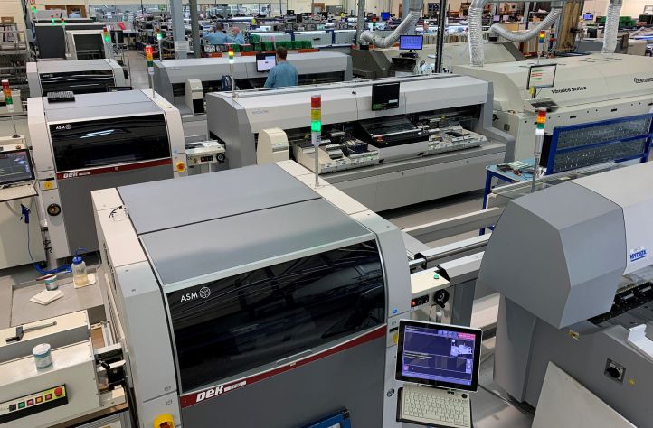
- Five SMT lines, each containing DEK 03iX Solder printers, Mycronic MY300DX SMT placement machines and 10 zone reflow ovens, with Air, Nitrogen capabilities, as well as Air-Nitrogen vacuum assisted convection reflow for void free power electronic soldering
- ASSCON VP6000 Vacuum Assisted Vapour Phase reflow oven
- 2 off Koh Young ZENITH 2 3D Automatic Optical Inspection (AOI) systems
- 2 off TAKAYA APT1400F flying probe test systems
- 1 off DAGE QUADRA 5 X-Ray system with CT scan capability
- 1 off NORDSON NOVO 460 PD Selective Soldering System
- 1 off LPKF Microline 2120P Laser de-panel system
- 1 off CENCORP SR1300 Automatic PCB de-panel system
- 100 staff

CIL’s five SMT production lines each capable of placing 01005 and CSP components coupled with advance 3D AOI / Flying probe test / X-Ray / CT Scan / Functional test / Laser and Auto PCB de-panel systems and gives CIL one of the most advanced PCBA assembly and test facilities in the UK. An area of specialisation that CIL has worked on is the assembly of power PCBA soldered in a vacuum for near void free assemblies which is an absolute essential requirement when dealing with GaN and SiC packages. The investment in the ASSCON VP6000 Vacuum assisted vapour phase was the first innovation for batch related work, but as CIL now works towards higher volumes it has added an in-line SMT Maschinen GmbH 10 zone Air/N2 convection reflow oven with vacuum assist to one of its SMT lines. When coupled with on-site X-Ray / CT Scan / CSAM this gives CIL an un-rivalled process capability for the manufacture of almost void free power electronics.
A combination of the new micro-electronics, power device and volume manufacturing facility and its existing enhanced facility will result in CIL being the most advanced electronics development and manufacturing company in the UK. CIL will be able to process from wafer dicing, device packaging, PCBA assembly, inspection, functional test and full product manufacture. This capability and capacity will enable both its existing customer base to realise their growth potential and also position CIL as a central enabler in the “Driving the Electric Revolution” “Net Zero” solution for a greener future.