CIL's ADVANCED SEMICONDUCTOR PACKAGING FACILITY UPDATE
It's been 6 months since CIL announced it's newly created and UK based advanced semiconductor packaging facility. Contained within the 46,000sq ft facility is a 15,000sq ft ISO7 (Class 10,000) fully qualified cleanroom that is starting to come on line and will be ready by late May 2023.
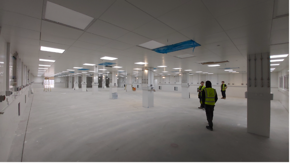 15,000sq ft ISO7 Cleanroom ready for anti-static floor install
Since last announced, CIL has also taken the decision to segregate part of this cleanroom to add a separate wafer dicing area complete with DISCO DAD3361 dicing saw and all of the necessary ancillary equipment. This equipment is already installed, commissioned and currently running early engineering trials. This wafer dicing equipment and all of CIL’s current micro-electronics and power semiconductor device packaging equipment will then start to transfer out of CIL’s existing facilities in Andover UK from late May 2023 onwards. The equipment and facilities to be transferred are initially the following:
- 1 off DISCO DAD3361 die and device wafer saw system complete with wafer mounting equipment.
- 2 off DATACON 2200EVO Automatic die bonders for power die placement using both SiC & GaN
- 2 off Automatic die bonders
- 2 off manual die bonders
- 5 off ASM 589 Automatic Al wedge bonders
- 2 off ASM EAGLE60 Automatic Au Ball bonders
- 1 off K&S Asterion Heavy Gauge Wedge wire bonder
- 1 off DAGE 4000 die shear/wire bond pull tester
- 1 off DAGE PROSPECTOR die shear/wire bond pull and full diagnostic test system
- 2 off Nordson Asymtek S2-920 Auto dispense systems for auto partial glob top
- 1 off DAGE Quadra7 X-Ray/CT Scan system.
- 1 off Nordson GEN7 Scanning Acoustic Microscope (CSAM)
- 1 off Keyence VHX7000 Digital Microscope with sub-micron laser measurement
- 1 off Boschman Sinterstar Innovate F-XL sinter press for high pressure silver sintering
- 1 off Boschman Pre-heat and cooling tower system for high pressure silver sintering
- 1 off Boschman UNISTAR Auto plastic overmold machine. Capable of BGA’s, LGA’s, QFN’s, Plastic IC’s, Power discrete and Power modules
- 1 off Scheugenpflug VDS U1000 / LP804 VDU Auto epoxy fill system
- 1 off high power 2000W laser welding system for copper busbar welding
- 6 off 3D Printers
- 50 staff of which 30 are engineers
CIL believes this facility, process equipment and staff will create the largest semiconductor packaging facility in the UK. It is to support and grow its existing micro-electronics customers and to commercially exploit its WBG power semiconductor capability that has been generated from various “Net Zero” low carbon projects funded by APC / InnovateUK / DCMS / BEIS using the latest SiC and GaN devices as well as commercially funded projects.
By adding the wafer dicing capability to the facility, CIL will be able to process finished wafers to provide Dicing, Die attach, Wire bonding or power device copper clip attach, glob top, full plastic overmold or potting and back these processes up with inspection equipment that includes, X-Ray, CT-Scan, CSAM, VHX7000, and destructive and non-destructive testing using DAGE 4000 and DAGE PROSPECTOR test stations.
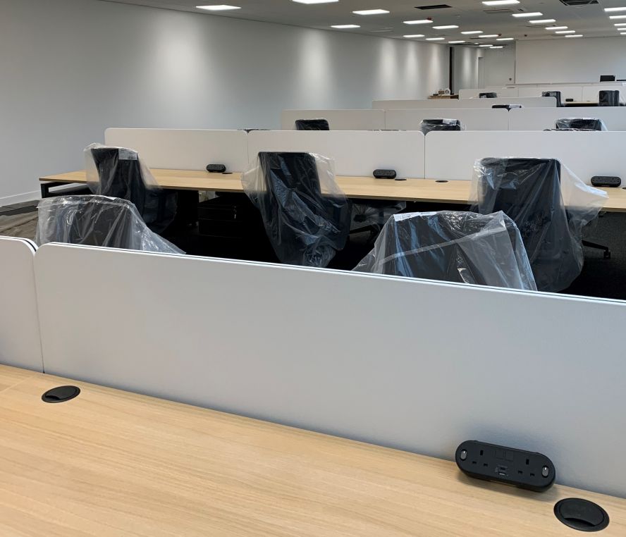
New offices for initial 32 Engineers
Over the last 3-4 years CIL has grown its engineering department from 8 persons to the 32 persons it has currently and also has a further 10 engineering vacancies. Starting in late May 2023, all of the staff involved in CIL’s semiconductor and power packaging activities will move from CIL’s two existing facilities into this new world class and state of the art semiconductor packaging facility. As with the cleanroom, the offices are nearing completion and will initially house around 30 semiconductor packaging engineers of all levels.
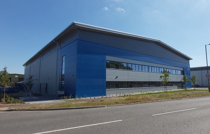
CIL Advanced Semiconductor packaging facility
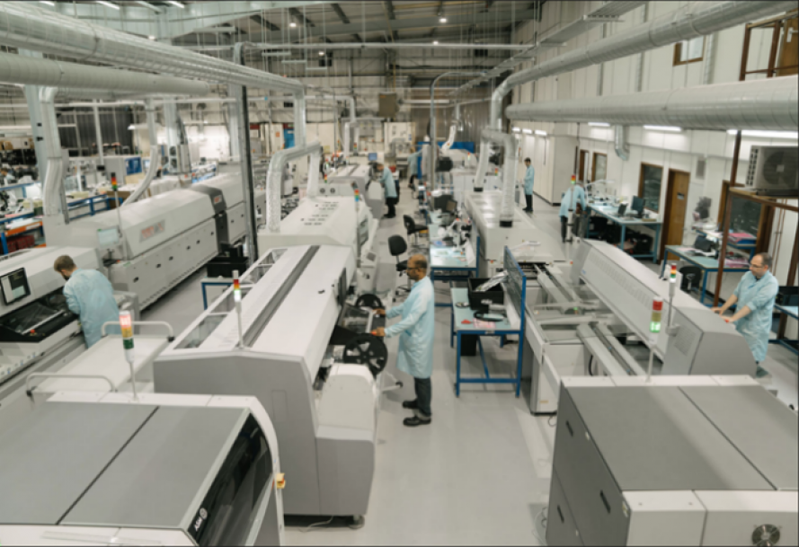
To compliment this semiconductor packaging facility, CIL has also upgraded its existing SMT PCBA equipment consisting of 5 SMT lines and associated 3D AOI, Flying probe test and IPC2 / 3 soldering at its CIL House facility also in Andover UK. This facility totalling 24,000sq ft is being steadily upgraded and added to.
In the last 2 years, CIL has seen its turnover increase from £15M to £27M and headcount increase from 135 persons to 187 persons it has today. Over the next 12 months, as well as bringing on line its advanced semiconductor packaging facility, it will also be adding new processes and equipment to its current PCBA service offering to further support both its customers development and production needs. So with the new packaging facility this will give CIL a total of 80,000sq ft of production space at its three Andover UK sites.
More news to follow
